Discover our complete solutions portfolio covering Cathodic Protection and Corrosion management - PCB design and plating - Functional and decorative plating - Electrocoating - Acoustics
Discover Protect
Elsyca V-PIMS
A revolution in digital PIMS combining Pipeline Corrosion Integrity Management System (PIMS) and computational modeling capabilities
Elsyca IRIS
Deep analysis of AC threats supporting efficient mitigation systems computer-aided design
Elsyca CatPro
Graphical simulation platform for cathodic protection and DC stray current analysis of pipeline networks
Elsyca CPManager
3D CAD-based software simulation platform for the computer-aided design and analysis of cathodic protection installations
Elsyca ACTA
Unique solution offering accurate, disambiguated, and tailored risk ranking report of pipeline networks
Plate
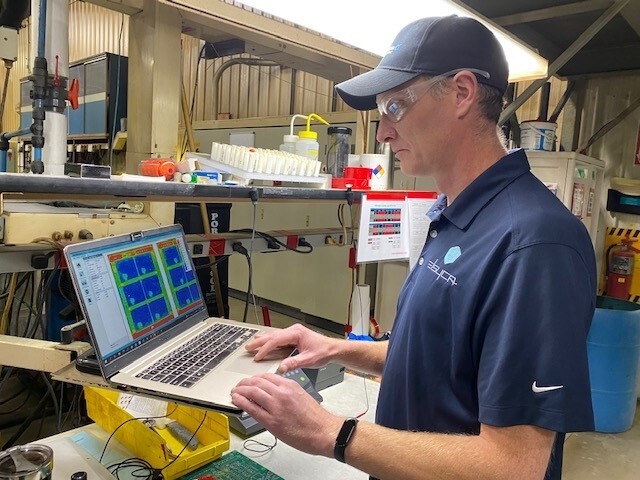
Elsyca PlatingManager
Leverage a digital twin of your plating line to predict plating performance and increase manufacturing capacity
Elsyca PCBBalance
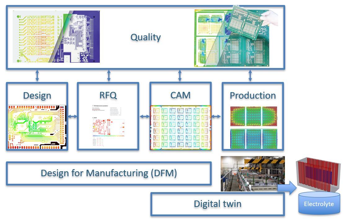
The world’s only PCB DFM software that applies automated and optimized copper balancing to your PCB design and panel layout.
Elsyca PCBPlate
State-of-the-art graphical simulation platform for enhancing the plating performance of your PCB panel and pattern plating processes.
Elsyca ECoatMaster
CAD independent software platform for the simulation of the automotive electrocoating process of a body-in-white (BIW).
Elsyca EPOS
Simulate the performances of electropolishing processes based on a virtual mock-up of the electropolishing cell.
Elsyca AnodizingManager
State-of-the-art graphical simulation platform for analyzing the production performance and quality of anodizing processes.
Innovate
Elsyca CorrosionMaster
CorrosionMaster identifies corrosion hot spots and predicts corrosion rates, enabling engineers to look at alternative material combinations and/or coating systems, or investigate corrosion-mitigating measures.
Elsyca LeakageMaster
Improve vehicles interior acoustic comfort by performing upfront virtual smoke tests.
Elsyca MeshingMaster
Automatically creates meshes for a variety of applications such as acoustics, CFD, thermal analysis, etc
Elsyca XPlorer
Interactive simulation results viewer for Finite Elements results
Elsyca XPlorer3D
Analyze, Understand and Get Immersed in your results
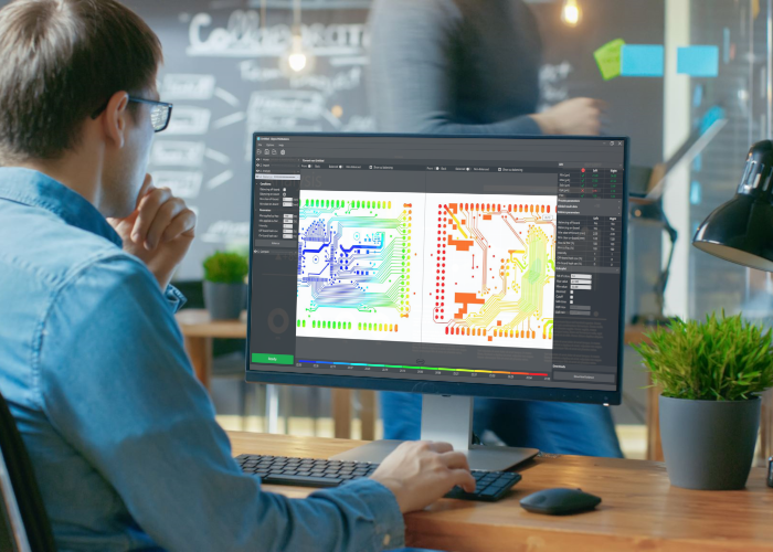
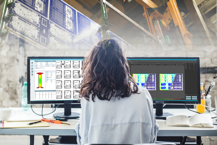
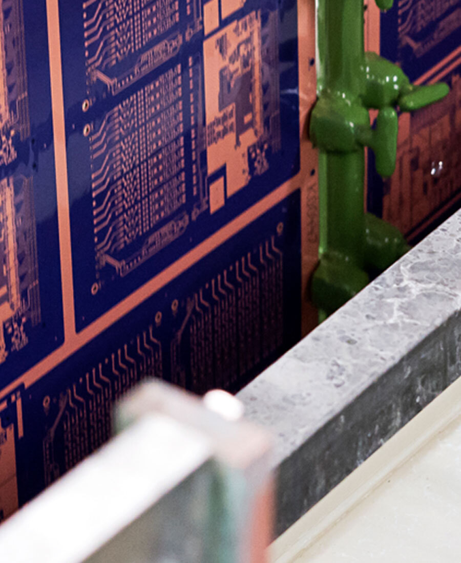
Our solutions for the PCB industry
" CEC’s use of the Elsyca software has helped to accurately predict the needed plating parameters to increase our first pass yields on new parts. "
" Copper balance and thickness uniformity reduces scrap rate and improves yield. Nowadays with advanced technology, such software is strongly recommended "
" Copper balancing should be done, not only at the panel level in PCB FAB, but every PCB designer should be taught the many benefits of copper balancing and incorporate the concepts into their board designs "
" Elsyca software helps us a lot to identify critical areas already in the design phase. But we also can use it on the shop floor to support our Engineers to predict how different set ups of designs and parameters influence the outcome. Due to this fact we can reduce the amount of trials which also leads to cost reduction. "