












August 7, 2026
Elsyca Webinar
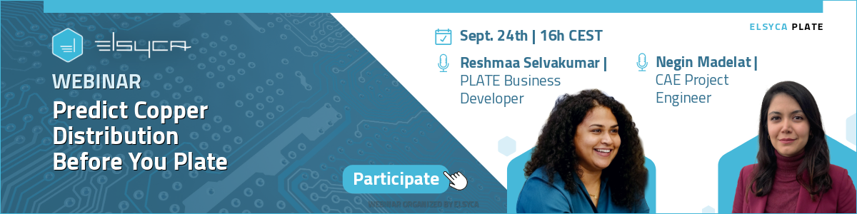
📅 Thursday, September 24th at 16h CET
📍 Virtual Event
Copper electroplating is one of the most sensitive steps in PCB manufacturing. Small changes in panel layout, load, chemistry, or rectifier settings can flip you from in-spec to scrap, and uneven thickness, hotspots, and under-plated regions stay invisible at the design stage until they surface on the line as cost, delays, and reliability risk.
This session shows how Elsyca PCBStudio lets you predict copper distribution before you plate, walking through a real board from Gerber import to a production-ready, validated setup.
You'll Learn
In this webinar, Elsyca will show how PCBStudio allows you to:
▪️ See finished copper thickness distribution across every board on the panel before production.
▪️ Automate copper balancing with patented algorithms to generate optimized patterns fast.
▪️ Spot plating risks and thickness issues that standard DFM tools don't show.
▪️ Reduce scrap and protect margins with fewer out-of-spec panels and less rework.
▪️ Deliver boards faster by preventing redesign loops and last-minute surprises.
▪️ Compare layout options on objective KPIs and enter production with confidence.
Who Should Attend
🔹 PCB Manufacturing & Process Engineers.
🔹 OEM & PCB Layout Designers.
🔹 CAM and Pre-Production Engineers.
🔹 Quality, Yield & Reliability Leads.
🔹 Plating Line & Production Managers.
🔹 R&D and DFM Specialists.
Save Your Seat Today!
Join us to see how simulation lets you catch plating problems before a single panel is run, cut scrap, and enter production with a setup already proven to work.