
Discover our complete solutions portfolio covering Cathodic Protection and Corrosion management - PCB design and plating - Functional and decorative plating - Electrocoating - Acoustics
Discover Protect
Elsyca V-PIMS
A revolution in digital PIMS combining Pipeline Corrosion Integrity Management System (PIMS) and computational modeling capabilities
Elsyca IRIS
Deep analysis of AC threats supporting efficient mitigation systems computer-aided design
Elsyca CatPro
Graphical simulation platform for cathodic protection and DC stray current analysis of pipeline networks
Elsyca CPManager
3D CAD-based software simulation platform for the computer-aided design and analysis of cathodic protection installations
Elsyca ACTA
Unique solution offering accurate, disambiguated, and tailored risk ranking report of pipeline networks
Plate
Elsyca PlatingManager
Leverage a digital twin of your plating line to predict plating performance and increase manufacturing capacity
Elsyca PCBBalance
The world’s only PCB DFM software that applies automated and optimized copper balancing to your PCB design and panel layout.
Elsyca PCBPlate
State-of-the-art graphical simulation platform for enhancing the plating performance of your PCB panel and pattern plating processes.
Elsyca ECoatMaster
CAD independent software platform for the simulation of the automotive electrocoating process of a body-in-white (BIW).
Elsyca EPOS
Simulate the performances of electropolishing processes based on a virtual mock-up of the electropolishing cell.
Elsyca AnodizingManager
State-of-the-art graphical simulation platform for analyzing the production performance and quality of anodizing processes.
Innovate
Elsyca CorrosionMaster
CorrosionMaster identifies corrosion hot spots and predicts corrosion rates, enabling engineers to look at alternative material combinations and/or coating systems, or investigate corrosion-mitigating measures.
Elsyca LeakageMaster
Improve vehicles interior acoustic comfort by performing upfront virtual smoke tests.
Elsyca MeshingMaster
Automatically creates meshes for a variety of applications such as acoustics, CFD, thermal analysis, etc
Elsyca XPlorer
Interactive simulation results viewer for Finite Elements results
Elsyca XPlorer3D
Analyze, Understand and Get Immersed in your results
PCB Plating: What every PCB Designer should know
Learn how you can improve design for manufacturing by considering PCB plating within your design cycle
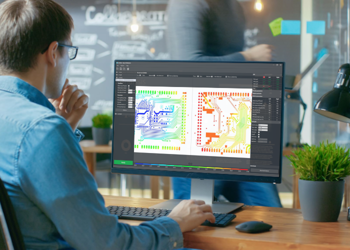
PCB Plating: What every PCB Designer should know
Context
In a previous post, we introduced the Elsyca CAE framework for a shift-left/shift right approach, a dedicated framework to ensure plating quality over the entire PCB design and manufacturing chain, improve design for manufacturing to ultimately reduce production costs.
But what is actually PCB plating and why PCB designers should consider it in the early design stages to ensure no plating issues are faced down the road?
So what is PCB Plating?
PCB plating is the process used to deposit the ten microns thick layer of copper on the board. This step is one of the numerous manufacturing steps required to build a PCB and is crucial as it gives the PCB boards its key role in conducting electrical signals in-between components.
With PCBs becoming thinner and more lightweight, ensuring the right width and thickness of copper layer while making sure that PCBs improve their signal integrity, efficiency, heat absorption capability and durability is a design and manufacturing challenge. Furthermore, PCB plating is a process sensitive to local conditions. The final layer thickness over the different boards is not homogeneous and produced boards might not meet specifications due to extra or insufficient deposit.
Having the ability to, as early as possible, verify that a new PCB design can actually be plated within specifications is a tremendous gain for OEMs and PCB designers as it shortens overall development cycle and reduces production costs.
An additional task for the designers?
PCB designers do already have to cope with a lot of technical requirements and challenges. Adding the integration of upfront plating feasibility within an existing design process should be done ingeniously in order to limit user operations and focus on providing the relevant insights when it is needed. PCB designers should be able to know when there is a potential threat, where it is located in their design, and what solutions they can apply to solve it.
Elsyca's solution focuses on delivering PCB designers a fast assessment of their designs with respect to plating based on standardized input files. The flexible API capabilities of the software allow for an automated and tailored integration within existing design processes. Our patented solution provides a unique approach able to consider the 3D effects of the holes on the final copper thickness, show user-defined KPIs, and suggest an optimized copper balancing all at once.
A significant benefit!
Being able to know early in the design stage if designs can actually be manufactured according to the highest requirements of quality and manufacturing yields is a major step forward in design for manufacturing. It goes behind the ability to avoid quality issues but also provides significant cost reduction together with energy consumption and material waste reduction.
Safran testifies that adding this solution to their existing process will help them make savings from 5% to 15% depending on the complexity of the designs. Within a context where RAW material prices and in particular copper foil prices are going up, the ability to avoid material waste while ensuring faster go-to-market delivery is key for more being more competitive.
What the future holds?
With PCBs becoming thinner and more lightweight, designers and manufacturers need to rely on solutions ensuring them that the right width and thickness of copper layers are deposited while making sure signal integrity, efficiency, heat absorption capability and durability are not compromised.
The ability to verify as early as possible within the design cycle all aspects of manufacturing will accelerate the deployment of innovative and more effective solutions.