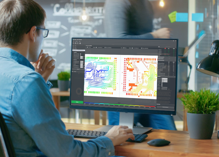
PCB Plating: What every PCB Designer should know
Learn how you can improve design for manufacturing by considering PCB plating within your design cycle

PCB Plating: What every PCB Designer should know
Context
In a previous post, we introduced the Elsyca CAE framework for a shift-left/shift right approach, a dedicated framework to ensure plating quality over the entire PCB design and manufacturing chain, improve design for manufacturing to ultimately reduce production costs.
But what is actually PCB plating and why PCB designers should consider it in the early design stages to ensure no plating issues are faced down the road?
So what is PCB Plating?
PCB plating is the process used to deposit the ten microns thick layer of copper on the board. This step is one of the numerous manufacturing steps required to build a PCB and is crucial as it gives the PCB boards its key role in conducting electrical signals in-between components.
With PCBs becoming thinner and more lightweight, ensuring the right width and thickness of copper layer while making sure that PCBs improve their signal integrity, efficiency, heat absorption capability and durability is a design and manufacturing challenge. Furthermore, PCB plating is a process sensitive to local conditions. The final layer thickness over the different boards is not homogeneous and produced boards might not meet specifications due to extra or insufficient deposit.
Having the ability to, as early as possible, verify that a new PCB design can actually be plated within specifications is a tremendous gain for OEMs and PCB designers as it shortens overall development cycle and reduces production costs.
An additional task for the designers?
PCB designers do already have to cope with a lot of technical requirements and challenges. Adding the integration of upfront plating feasibility within an existing design process should be done ingeniously in order to limit user operations and focus on providing the relevant insights when it is needed. PCB designers should be able to know when there is a potential threat, where it is located in their design, and what solutions they can apply to solve it.
Elsyca's solution focuses on delivering PCB designers a fast assessment of their designs with respect to plating based on standardized input files. The flexible API capabilities of the software allow for an automated and tailored integration within existing design processes. Our patented solution provides a unique approach able to consider the 3D effects of the holes on the final copper thickness, show user-defined KPIs, and suggest an optimized copper balancing all at once.
A significant benefit!
Being able to know early in the design stage if designs can actually be manufactured according to the highest requirements of quality and manufacturing yields is a major step forward in design for manufacturing. It goes behind the ability to avoid quality issues but also provides significant cost reduction together with energy consumption and material waste reduction.
Safran testifies that adding this solution to their existing process will help them make savings from 5% to 15% depending on the complexity of the designs. Within a context where RAW material prices and in particular copper foil prices are going up, the ability to avoid material waste while ensuring faster go-to-market delivery is key for more being more competitive.
What the future holds?
With PCBs becoming thinner and more lightweight, designers and manufacturers need to rely on solutions ensuring them that the right width and thickness of copper layers are deposited while making sure signal integrity, efficiency, heat absorption capability and durability are not compromised.
The ability to verify as early as possible within the design cycle all aspects of manufacturing will accelerate the deployment of innovative and more effective solutions.
