
Discover our complete solutions portfolio covering Cathodic Protection and Corrosion management - PCB design and plating - Functional and decorative plating - Electrocoating - Acoustics
Discover Protect
Elsyca V-PIMS
A revolution in digital PIMS combining Pipeline Corrosion Integrity Management System (PIMS) and computational modeling capabilities
Elsyca IRIS
Deep analysis of AC threats supporting efficient mitigation systems computer-aided design
Elsyca CatPro
Graphical simulation platform for cathodic protection and DC stray current analysis of pipeline networks
Elsyca CPManager
3D CAD-based software simulation platform for the computer-aided design and analysis of cathodic protection installations
Elsyca ACTA
Unique solution offering accurate, disambiguated, and tailored risk ranking report of pipeline networks
Plate
Elsyca PlatingManager
Leverage a digital twin of your plating line to predict plating performance and increase manufacturing capacity
Elsyca PCBBalance
The world’s only PCB DFM software that applies automated and optimized copper balancing to your PCB design and panel layout.
Elsyca PCBPlate
State-of-the-art graphical simulation platform for enhancing the plating performance of your PCB panel and pattern plating processes.
Elsyca ECoatMaster
CAD independent software platform for the simulation of the automotive electrocoating process of a body-in-white (BIW).
Elsyca EPOS
Simulate the performances of electropolishing processes based on a virtual mock-up of the electropolishing cell.
Elsyca AnodizingManager
State-of-the-art graphical simulation platform for analyzing the production performance and quality of anodizing processes.
Innovate
Elsyca CorrosionMaster
CorrosionMaster identifies corrosion hot spots and predicts corrosion rates, enabling engineers to look at alternative material combinations and/or coating systems, or investigate corrosion-mitigating measures.
Elsyca LeakageMaster
Improve vehicles interior acoustic comfort by performing upfront virtual smoke tests.
Elsyca MeshingMaster
Automatically creates meshes for a variety of applications such as acoustics, CFD, thermal analysis, etc
Elsyca XPlorer
Interactive simulation results viewer for Finite Elements results
Elsyca XPlorer3D
Analyze, Understand and Get Immersed in your results
How to increase PCB plating quality consistency?
How today's new solutions and tools can accelerate the development, reduce go-to-market time, ensure consistent quality and reduce scrap rates?
How to increase PCB plating quality consistency?
An introduction to the shift-left approach
Ensuring the quality of a complex product in a complex manufacturing chain.
A PCB is a very complex product, squeezing a lot of very complex and dense networks to connect all processors, sensors, … all of these in a small footprint. A PCB network must transport the electrical signal from point A to B without failure. Electrical signal integrity is key to ensuring the final product operates as expected. In order to achieve a successful design, PCB designers will upfront analyze their design to avoid cross-talk, impedance issues, heat problems, ….
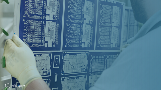
Once the design is done, the FAB will receive it together with specifications and are in charge of building the part to these requirements. During manufacturing, the deposit of copper on the board is a key step of the process that has typically very tight tolerances. This is done via electroplating and due to the nature of the process, the resulting copper layer thickness over the PCB will not be homogeneous.
It can even get worse: as multiple PCBs are produced at once, one will also have variations between the PCBs, even if they do have the same design. The FAB will do its best to keep these variations under control.
Assessing plating quality.
The typical methodology used to validate the plating process is to build parts and measure the final plating quality. Not only this process requires time, and money and will therefore slow down the start of production, but it also brings additional constraints. Indeed, the only real measurement is a destructive one and consists in making cross-sections in a PCB.
In order to avoid destroying the product they want to sell, FAB will typically use what is called test coupons. Test coupons are areas on the panel, outside of the PCB locations, that contain holes or a small pattern and can be used for cross sections without losing any PCBs. A critical drawback of this approach is that a test coupon is typically positioned in irrelevant areas. Therefore, the information obtained at its location only provides for the test coupon itself and is actually not representative of the thickness over the PCB. The copper layer thickness on PCBs, even only a few cm away from a test coupon, can be completely different. This is quite a dilemma.
Start early, save a lot!
It is common knowledge that the cost to fix a problem is relatively low when detected earlier in the process. When it comes to PCBs, the first thing to make sure is that specifications are clearly stated, complete and agreed with all stakeholders. These specifications must also be realistic, with an eye on both design and production constraints as well as expected and/or possible quality. Clearly, the final details will only be known at the end, but the more you can identify at the start, the more effective and efficient the following process steps will be.
Problem is, that not all steps are done by the same team or company. Consider you are an AOEM, and want to include a lane assist functionality in your new vehicle. You will create the specifications, and find a company to provide e.g. the radar/lidar devices. This will be provided by a tier 1 supplier, who will design the part and the PCB design, but will also outsource PCB manufacturing. The PCB manufacturing company may do the assembly, but outsource the bare board manufacturing to another company. Just imagine this last company identifies a problem that requires a design change in order to produce the part to spec. How much time will be lost before this ‘ripples back’ to the original designer and how expensive it will be to fix the issue.
This can be avoided using a Shift-Left approach: at each step of the process, one verifies to the extend possible that the outcome of the current process can be used by the next step(s).
What about computer aided engineering?
The use of Computer Aided Engineering (CAE) solutions is a no-brainer to test all type of mechanical aspects/integration in e.g., the development of a car, but is not yet adopted as standard when developing new PCBs moreover when it comes to the plating aspect of the PCBs.
As for other industries, an upfront validation (shift left approach) not only saves a lot of time, but also cost. Safran reports a +10% reduction on their PCB cost using simulations to validate and optimize their PCB design for copper layer thickness uniformity. In a very cost-aware industry like OEMs, that is definitely something to explore in an accelerated rate!
But how does this works for the different steps related to PCBs? Let's try to have a look for the different stakeholders:
- Designer: PCB designers can use simulation to compute the expected copper layer thickness variations over a board. This provides crucial information for the designer to identify regions with problematic values (high/lows), and even receive automated and optimized copper balancing suggestions (without touching the original design). Just think about the time that is lost if these design problems are only detected and (in best case) reported back by the FAB, compared to validating your design in a few minutes time.
- RFQ: As for PCB designers, sales team can start with same software to upfront validate if a design will be a potential problematic part. This provides solid input for the offer to define a correct price, allows to provide feedback to the designer, and avoids unpleasant surprises in production.
- CAM: The panelization step is a crucial factor in the process as this has a direct impact on your production capacity and quality. CAM engineers can validate the panel layout on their own, resulting in objective and easy to interpret overview of the layer thickness distribution. KPIs will be shown based on the board areas only. Copper balancing between the boards can be automated and is optimized towards the panel/board layout (and far more effective compared to the build in ‘fill this rectangle with a hatch’ functionality offered in the standard CAM environments). This technology can also be integrated in CAM environment to create for example a single click ‘thumbs up/down’ functionality.
- Production: Production team members will be able to upfront validate a configuration. This will be based on a digital twin of the plating infrastructure and electrolyte. A trial-and-error run in the virtual world will take about 1 hour, including setup, simulation and analysis. The simulations provide full details on the entire panels, not only on the surface, but also including holes.
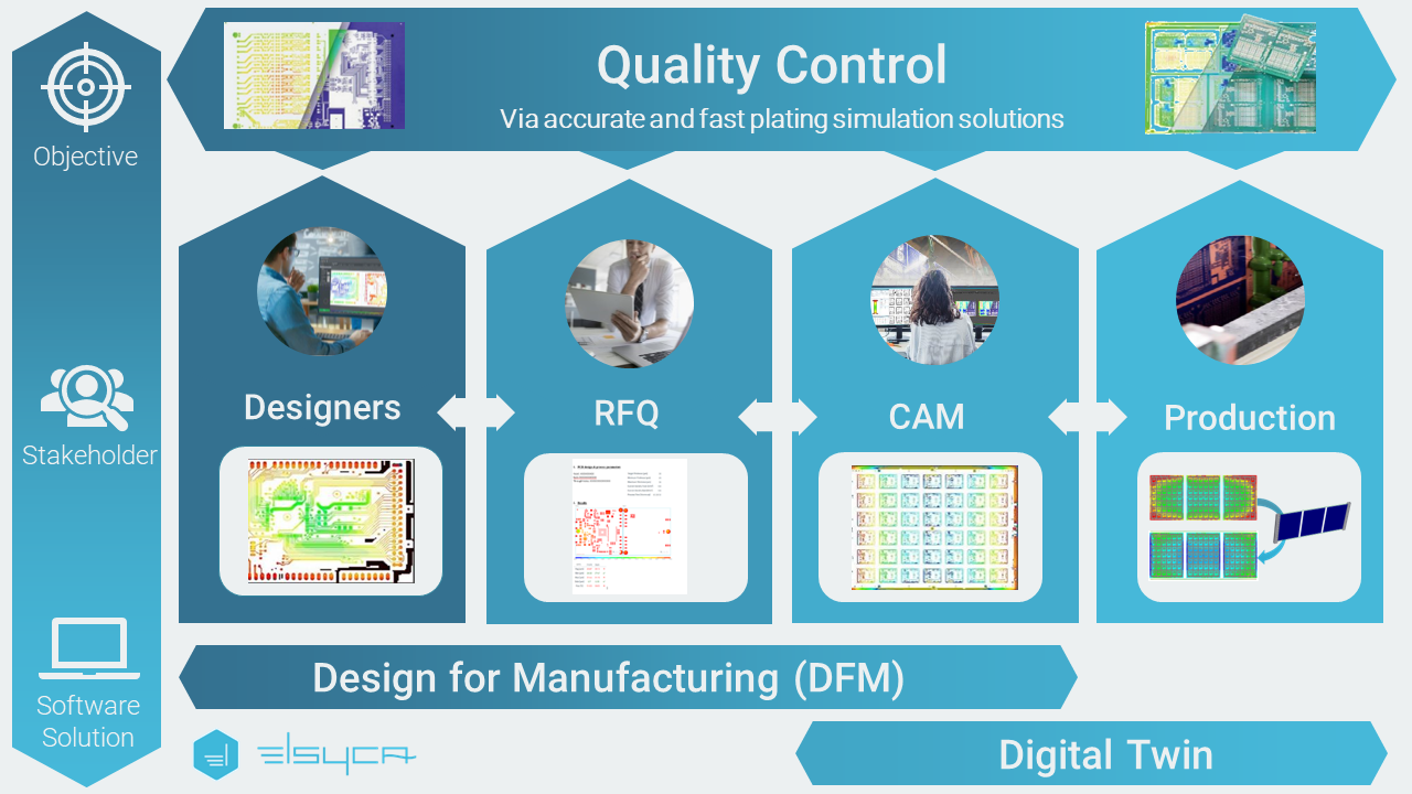
Thanks to this approach, the overall quality control is more effective and efficient as:
- Simulation identifies the hotspots, so we know what/where to test.
- The use of test coupons is now ‘magnified’: a cross section of a test coupon is often required to provide proof boards are within specification. It is however very likely that the values – even only a few cm further – may be drastically different. With simulations, the simulated/measured values of the test coupon can be used as a benchmark for accuracy, and use this to validate ALL other values on panels.
What's next?
The adoption of a CAE solution within an existing design or manufacturing process might seem complex and cumbersome at first, do not worry it is not. Our team of experts is here to guide every stakeholders with best practices, tailored to their needs, existing solutions and specific infrastructures.
Elsyca team support the integration of automatic copper balancing within existing ECAD environment so that PCB designers can keep the focus on their work. Specialized CAE engineers do collaborate with FAB owners and engineers to develop turnkey digital twin models of their plating lines to make sure that every required information, including geometrical and electrochemical aspects, are considered.
Do not wait to Elsyca-lize your process in order to save time and money while gaining insights on and competitiveness!
Download the overview
You can download the overall process overview infographics via the below button.
Would you be interested in knowing more about Elsyca's solutions that can help you shift-left your PCB quality insurance approach, do not hesitate to contact us!