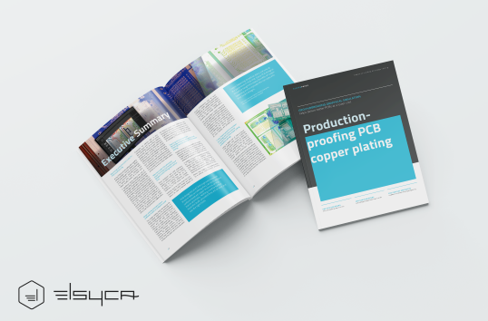
Production-proofing PCB copper plating
An introduction to new exciting computer simulation technology for PCB CAM, production, and design engineers to validate plating thickness and automatically add copper balancing

How a groundbreaking graphical simulation helps deliver better PCBs at a lower cost.
As the PCB industry is coping with ongoing miniaturization, shorter delivery times, and profit margins that are increasingly under pressure, manufacturers need to deliver ever more complex and higher quality boards at a lower cost.
A significant factor affeing the cost of manufacturing PCBs is production yield, the percentage of manufactured PCB panels that meet specifications. Especially highend PCBs stretch production processes to their limits, resulting in more out-of-spec products. Therefore, increasing production yield through better control of the different production steps is an absolute necessity for every PCB production manager. But as the outcome of the production process depends on the PCB design and the panel layout that is committed to production, increasing production yield can only be achieved through a joint effort of all PCB production stakeholders.
In this white paper, we explore all PCB plating related challenges PCB designers, CAM engineers and process engineers are facing thoughout the PCB design and manufacturing process and how Elsyca’s graphical simulation technology makes the difference between knowing or guessing.
Request our white paper here and read more about these NEW simulation tools for PCB and panels.
