
Discover our complete solutions portfolio covering Cathodic Protection and Corrosion management - PCB design and plating - Functional and decorative plating - Electrocoating - Acoustics
Discover Protect
Elsyca V-PIMS
A revolution in digital PIMS combining Pipeline Corrosion Integrity Management System (PIMS) and computational modeling capabilities
Elsyca IRIS
Deep analysis of AC threats supporting efficient mitigation systems computer-aided design
Elsyca CatPro
Graphical simulation platform for cathodic protection and DC stray current analysis of pipeline networks
Elsyca CPManager
3D CAD-based software simulation platform for the computer-aided design and analysis of cathodic protection installations
Elsyca ACTA
Unique solution offering accurate, disambiguated, and tailored risk ranking report of pipeline networks
Plate
Elsyca PlatingManager
Leverage a digital twin of your plating line to predict plating performance and increase manufacturing capacity
Elsyca PCBBalance
The world’s only PCB DFM software that applies automated and optimized copper balancing to your PCB design and panel layout.
Elsyca PCBPlate
State-of-the-art graphical simulation platform for enhancing the plating performance of your PCB panel and pattern plating processes.
Elsyca ECoatMaster
CAD independent software platform for the simulation of the automotive electrocoating process of a body-in-white (BIW).
Elsyca EPOS
Simulate the performances of electropolishing processes based on a virtual mock-up of the electropolishing cell.
Elsyca AnodizingManager
State-of-the-art graphical simulation platform for analyzing the production performance and quality of anodizing processes.
Innovate
Elsyca CorrosionMaster
CorrosionMaster identifies corrosion hot spots and predicts corrosion rates, enabling engineers to look at alternative material combinations and/or coating systems, or investigate corrosion-mitigating measures.
Elsyca LeakageMaster
Improve vehicles interior acoustic comfort by performing upfront virtual smoke tests.
Elsyca MeshingMaster
Automatically creates meshes for a variety of applications such as acoustics, CFD, thermal analysis, etc
Elsyca XPlorer
Interactive simulation results viewer for Finite Elements results
Elsyca XPlorer3D
Analyze, Understand and Get Immersed in your results
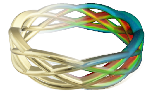
Challenges in decorative gold plating
Learn more on the challenges in decorative gold plating and how manufacturers can achieve a deposit thickness that resists wear without the need to overplate.
Context and challenges
A decorative gold surface finish is applied to many luxury items such as jewelry, watches, writing instruments and eyeglasses.
Decorative gold plating involves alloying gold with other metals such as copper or silver. Therefore, both appearance (yellow to red to white) and gold content of the deposit (carat or K) will depend on the plating bath (chemistry and aging of the bath) and process conditions (flow, current density), and can vary significantly over a single part and between parts.
From a manufacturing perspective, the challenge is to achieve a deposit thickness that resists wear and degradation without overplating and wasting the precious metal. This is very difficult for jewelry of complex design comprising recesses because, without any special tooling, when the deposit thickness is raised in the recesses, there is a significant overplating elsewhere – easily by more than 50%.
Elsyca has developed a unique technology that accurately predicts the thickness distribution of metal layers – no matter the complexity of the component. This allows the process and tooling to be optimized to control costs and quality.
A design plateability analysis on a bracelet shows the problem areas for meeting minimum layer thickness and karat specifications.
More about decorative gold plating
Decorative gold plating is widely used for luxury items such as rings, necklaces, watches, writing instruments, belt and purse fasteners and eye glasses. Depending on the alloying element incorporation the appearance of the deposit can range from red gold (alloy with copper) over yellow gold to white gold (alloy with silver). The gold weight fraction in the deposit is expressed as karat (K). Common gold weight fractions are 21K (87 w % Au), 18K (75 w % Au) and 14K (58 w % Au).
If the substrate is non-conductive (e.g plastic) than activation and electroless nickel or copper process steps are required for creating a conducitve seed layer. A copper and nickel layer will be plated prior to the final gold layer. This gold layer is often only a few micron thick. In case of metal substrates often also copper and nickel layers will be plated prior to the gold layer. When the substrate already consists of the copper alloy, the copper plating step might become obsolete
A special process is gold electroforming of jewels. This process allows creating voluminous jewels that are hollow at the inside and have a gold wall thickness of about 100 to 200 micron. This ensures that the structural rigidity of the gold shell is high enough, while the gold weight of the jewel is only a fraction of the same jewel that would be obtained through casting. The process starts with the casting of a mandrill or core in tin-bismut (low melting alloy). These cores are then mounted on a rack, next cleaned prior to going through an alkaline and an acid copper plating step. Finally the parts are gold plated for a sufficiently long time (5 – 15 hours) in order to obtain a sufficient gold layer thickness. The tin-bismut core is removed by a heated centrifugal process through a hole in the old schell, next the inner copper layer is removed by acid etching.
Although the throwing power of most gold baths is moderate to good, the weight of over-plated gold on a part in order to reach minimum thickness specifications in recessed areas can amount to over 50 % of the minimum weight that would be required theoretically. This is not really a problem for gold electroformed jewels as their price is based on the gold weight, added a fixed manufacturing cost, but it poses a serious problem for decorative gold surface finishing of larger size jewels with a complex geometry. The throwing power also rapidly declines when the average applied current density is increased, hence decorative gold plating baths are operated at very low current density values, typically 40 – 150 A/m2 (4 – 15 ASF).
A second problem with gold plating baths is that the alloy content in the deposit depends on the current density and flow conditions. Typically the gold content will decrease with current density and increase with flow. In addition, the alloy content will also depend on the bath chemistry and aging. As a result, the gold weight fraction in the deposit can vary over a single part and from part to part, with the risk that parts are plated with a gold deposit that does not meet the specified karat level (hence the production of scrap parts). In summary, recessed surface areas on a part that receive a low current density value are likely to have a gold deposit thickness below specifications, whereas protruding surfaces areas (edges) will receive high current density values and risk to be plated below minimal gold content (K) specifications. This means that in the end the plater is left with a pretty narrow operational current density window.
Elsyca's solutions
Elsyca's Advanced Engineering Services (AES) for decorative gold plating are manifold, starting with the laboratory characterization and sensitivity analysis of the different gold plating baths. This not only provides essential data that enables us to accurately predict gold plating thickness distributions but provides an unparalleled insight into the process, clearly defining the optimum window of process operating conditions. Additional characterization of copper and / or nickel plating steps that precede the actual gold plating step should also be executed.
- A design plateability analysis is a very quick analysis process that can be adopted by an OEM to decide on the degree of over plating that is required in order to bring the recessed surface areas above minimum thickness specifications.
- A rack plateability analysis provides a fast plating performance analysis of a part and tooling configuration as specified by the customer, for a rack that is either intended to be built, or that is running in a test phase or in production.
A Computer Aided Engineering (CAE) project for the decorative old plating process of a specified part program will target to obtain the best possible part configuration and load on a rack. In addition tooling conponents are defined and optmised. These will often include an integrated configuration of shields, current robbers and/or conforming anodes. The Computer Aided Engineering (CAE) work relies upon computer simulations for obtaining the current density, layer thickness and alloy content distribution over the parts. The tooling configuration is iteratively improved based on the simulations results while accounting for all possible practical restrictions with respect to manufacturability, hardware cost and maintenance issues.
Simulations are based on in-house developed software platforms, in casu Elsyca PlatingManager for the current density and layer thickness distribution simulations.
For projects that involve the CAE of an optimised tooling configuration, Elsyca optionally delivers also the CAD of the entire rack skeleton, including technical drawings and Bill of Materials.